1-805-484-2992
Quotes - Engineering - SalesAdvantage Chillers for Semiconductor Fabrication
Sub-micron semiconductor processes demand extreme thermal precision to control overlay, CD uniformity, and defect density. Advantage ultra-pure chillers deliver 1822°C (±0.03°C) DI water and 4080°C (±0.1°C) Galden® PFPE to EUV scanners, track systems, and diffusion furnaces using dual-redundant filtration, ion-exchange resin beds, and non-metallic fluid pathspreventing particle contamination and ensuring 99.999% tool uptime in ISO 3 cleanrooms.
Applications
- EUV Lithography Scanners: Chillers stabilize immersion hoods and projection optics at 22.000°C ±0.02°C, achieving -1 nm overlay and supporting 3 nm node production at 250 wph.
- Plasma Etch Chambers: Dual-loop systems cool 300 mm electrostatic chucks to 1060°C, maintaining etch rate uniformity -1% across wafer and preventing polymer buildup.
- ALD &CVD Reactors: PFPE chillers control pedestal temperatures from 350550°C with ±0.5°C ramp rates, enabling atomic-layer precision in high-k and barrier film deposition.
- RTP &Diffusion Furnaces: High-flow DI systems remove 80 kW from quartz tubes, stabilizing spike anneals at 1050°C ±1°C for dopant activation in logic and memory.
- Wafer Handling &Metrology: Point-of-use chillers maintain 21.0°C ±0.05°C in FOUPs and inspection stages, preventing thermal-induced wafer bow and measurement drift.
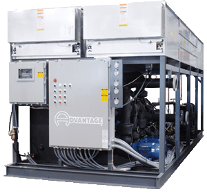
OACS Central Chillers
Outdoor Air-Cooled Systems
- 10500+ Ton Capacity
- Scroll or Screw Compressors
- Weatherproof NEMA 4X Controls
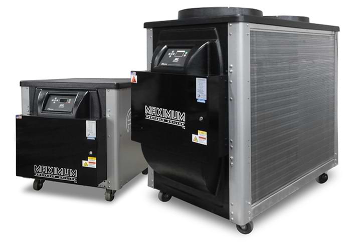
MG Series Portable Chillers
Packaged Air-Cooled Units
- 240 Ton Range
- Non-Ferrous Plumbing
- Digital Scroll
The Benefits of Advantage Chillers for Semiconductor Fabrication
In advanced node fabs, thermal control is the foundation of yield and cost-per-wafer. A leading logic foundry faced 3% yield loss from overlay drift in their EUV layer due to chiller instability. After installing an Advantage 300-ton ultra-pure DI central plant with dual 0.02 µm filters and predictive particle monitoring, they achieved ±0.018°C across 48 scanners, recovered 2.8% yield, reduced particle adds to <50 per wafer, and saved $42M annually in 3 nm production.
Advantage semiconductor chillers are built with electropolished 316L stainless fluid paths, perfluoroelastomer seals, and zero-copper wetted components to meet ITRS roadmap purity specs. PLCs with SECS/GEM II and 300 mm AMHS integration provide real-time process interlocks, while dual redundant pumps, compressors, and auto-changeover ensure zero unscheduled downtimeeven during facility power blips. Optional heat recovery captures 60% of waste heat for cleanroom reheat, cutting fab energy use by up to 18%.
From R&D pilot lines to high-volume 3 nm/2 nm megafabs, Advantage delivers the precision, purity, and reliability required to push semiconductor manufacturing to its physical limitswafer after wafer, node after node.